Bad Vibrations

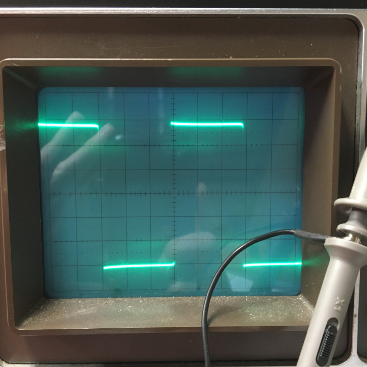
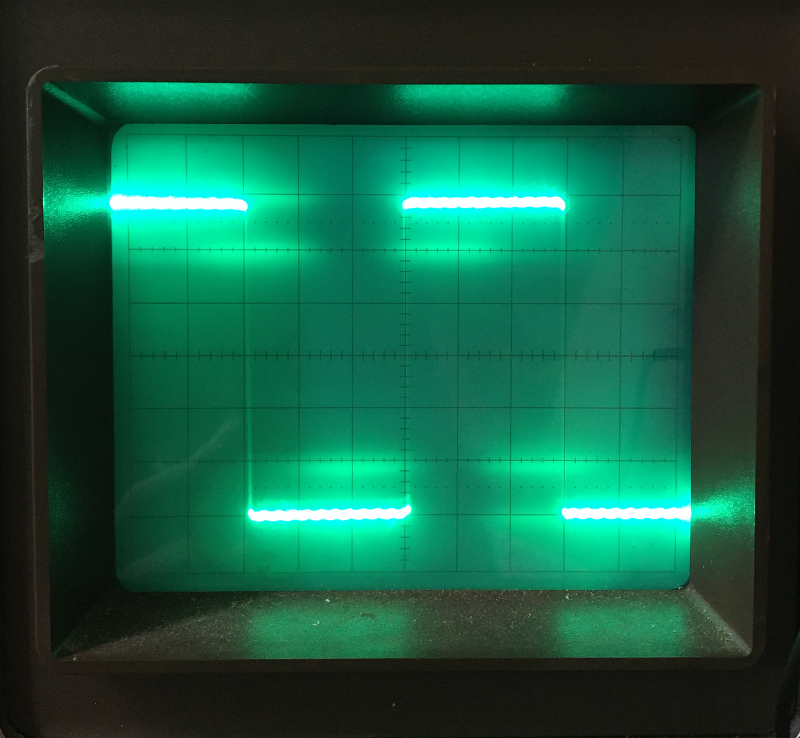
As the previous post hinted, I recently needed to fix my Phillips PM3217 oscilloscope. The problem? Bad vibrations. Or, rather, oscillations on the trace that just shouldn’t be there. Most all oscilloscopes have a test point on the front that is marked “cal” and has a hole to which you clip your oscilloscope probe. This test point provides a square-wave oscillation at a fixed frequency that you can use to adjust the compensation on the probe. I was doing just that when I noticed ripples on the square wave.

Not a great shot, but you can make out the ripples.

My first thought? Worn-out electrolytic capacitors in the power supply. Why? Probably because that would be the easiest problem to fix. Really, though, it’s a very common problem for electronics of every era. The first thing you should check is always the power supply.

Looking at the service manual, I discovered that the switch-mode power supply oscillates at about 18 kHz. That’s pretty close to the unwanted ripple, so that made me even more sure it was the power supply. Amazingly, my kid could hear the oscillation. I’m old enough that I can’t hear those frequencies, but young ears can!

So I opened up the case to take a look. The case opens up with two captive screws. That was refreshing. It’s like they expected you to fix your own equipment, so they made it easy to open. The power supply was easy to find. It’s in the back. A visual inspection turned up no leaking electrolyte, but that doesn’t mean the capacitors aren’t bad. I tested the ESR of each capacitor, and they were almost uniformly too high.

The power supply board

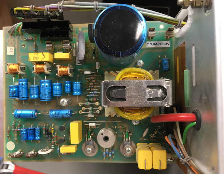
Thankfully I didn’t need to replace that huge cap at the top right. That cap filters the 120 Hz rectified AC input. Those usually aren’t the ones that fail first. It’s the smaller axial caps that are filtering the 18 kHz output. I replaced them with new axial caps, which cost a bit. Axial caps just aren’t popular anymore, so you have to pay a bit for new ones. I got them all from Vishay, from their industrial temperature, low ESR lines.

So did it fix the problem? You bet! Always check the power supply first!

That’s better, and a better picture! Turn down the intensity when taking CRT scope pictures.

Not Today, RIFA Cap!

Whenever buying or restoring an old piece of equipment, it is best to start with a good visual inspection. Burnt diodes or resistors, leaking capacitors, or melted-down tubes can mean that a component has failed, that the device was not operated as intended, or that it has been modified in an unsafe manner. But there are also pieces of equipment that are stock, in good condition, but which still have nasty surprises inside.

A RIFA capacitor, ready to fail.

One such nasty surprise are the radio frequency interference (RFI) suppression capacitors made by RIFA circa the 1980’s. These capacitors may be working fine when powered on, but they are ticking time bombs. The problem is the plastic enclosure: it develops cracks over time that allow moisture into the capacitor. The capacitor fails short, exactly what an X rated capacitor is not supposed to do, and causes some fantastic smoke to pour out of the equipment. The video below shows a successful attempt to document such a failure.

RIFA cap failure on a TRS 80 Model II, captured by Peter Cetinski

I found one of these RIFA caps inside of a Philips oscilloscope that I have had, and used, for years. I had no idea it was there until I saw it mentioned in a forum post about this particular oscilloscope. Rather than being on a circuit board, it is soldered directly to the back of the mains voltage selection knob at the back of the unit and hidden under a cover. If I hadn’t been looking for information about replacing the capacitors in the power supply section, I might not have found it until it failed.

All Sense of Proportion

I made a little breakout board for a chip I wanted to try out. It’s a current sense amplifier, so I put a spot for a shunt resistor to monitor. Can you spot the problem with my layout?

No? How about now:

Even if you had Lincoln’s tiny eyes you might have trouble making that out because text that size is at the limit of the silkscreen’s (or, probably, the inkjet’s) resolution. The software will zoom in with infinite resolution when you’re laying out the board, so there’s no warning when things get small. You have to keep track of the units. In this case, the text is 16 thousands of an inch.

WP-702A PSU Upgrade

I was working on an op amp circuit when it started to oscillate unexpectedly. I threw in more capacitance, took out capacitance, changed resistors, switched op amps, all to no avail. But then if changing your circuit doesn’t fix the problem then maybe the circuit isn’t the problem. Sure enough, it was the power supply that was oscillating. It looked just fine until you put a load on it. The other half of the dual supply failed at the same time, but it would just go dead as soon as there was a load. Maybe there was a spike on the AC line that fried them. Maybe it was the weather.

Crusty!

When I opened it up I was struck by how old the construction was and how crusty it had all become. The supply had been given to me by my grandfather years ago. I had assumed it was 80’s vintage but the dates on the meters were January 1972. It’s an RCA WP-702A, which appears to have continued production under the VIZ brand for many years. The design uses just 3 transistors and a few zener diodes per supply. The capacitors were clearly gone.

So it was time to learn about power supply design. I wasn’t going to throw this thing out, it’s just too handsome. So I decided to keep the transformer and front panel just as they were and design a drop-in replacement for the regulator boards, but with a slightly more modern design. I sketched out how the original circuit worked, mostly so I could get a handle on how the overload lights were switched on.


As far as I got with the existing circuit.

As you can see, turning on the overload light is pretty darn simple. They selected an incandescent bulb that begins to light at a current of 200 mA and wired it ahead of the pass transistor. All the current that comes out of the supply goes through the bulb first, and it lights itself at the maximum rated current.

So what about the new design? I decided to upgrade to the great granddaddy of regulator IC’s: the uA723. Created in 1967 by Bob Widler, it existed when this unit was manufactured, if not when it was designed.

My third pass.

This design includes ideas I got from others’ schematics, but I’m not sure all of them are good. The data sheet indicates, for example, that pre-regulating the voltage to the 723 improves ripple rejection, so I made a pre-regulator from a 24 V zener (D6) I already had and used one of the power transistors (Q1) as an emitter-follower. Is this a good place to put a capacitor to make it a capacitor-multiplier as well? I would suppose so, but I’m not sure how to calculate what value should be used. It would seem to need a big one to reject 120 Hz, and it reduces the ripple pretty darn well without it.

A bigger issue, perhaps, is how to get good regulation down to 0V. There are three resistors (R12, R13, R14) in the feedback loop that try to map the nominal 0 to 20 V output range onto the 2 to 7 V input range of the error amplifier. It works well enough with a load, but the voltage creeps up when the supply is unloaded. So I put some load resistors on both the 723’s output (R9) and the output of the external pass transistor (R15). I imagine giving the chip a negative supply helps with this by keeping 0 V in its normal operating range.

One idea that was definitely good was replacing the original one-turn pots on the front panel with ten-turn pots. A 20 V range on a one-turn pot is just too much. Also, I added a fuse to the primary side of the transformer. That combined with the over-current protection of the 723 (which I set at 250 mA) makes this thing a lot safer to use.

The PCBs returned perfect and purple, but I clearly made some goofs. Some of the footprints are just too big. (I intentionally left the second filter cap unpopulated.)

The finished PCB, installed.

All in all, I think this project turned out pretty well. The supply works, and that’s what’s most important. If it ever fails again, I’ll get to learn more about power supplies!

(No) Dummy

For a recent power supply project (more on that later) I needed a dummy load for testing. So I reached for my favorite Ohmite rheostat: 75 ohms with an approximate log taper and an off position. This is one I picked up at a hamfest real cheap. To test at the max voltage and current, I needed 100 ohms, however, so I added in a 25 ohm fixed wire-wound resistor for those tests. They worked really well, except they were just loose on the bench connected with gator clips that would sometimes slip off. So I built an enclosure for them.

Real Ohmite standoffs? Yes please!

The enclosure isn’t fully enclosed, as you can see. It consists of just two laser-cut pieces of acrylic with four 3″ 8-32 standoffs. The open sides allow the resistors some ventilation. It doesn’t have feet yet, but I plan to add non-marking rubber feet held on by the lower screws. I was pleased to find some short scraps of brightly colored solid wire in my junk bin.

I decided to add a scale for the rheostat. I did this by sketching up most of the layout in GeoGebra and then printing it out on paper. I poked the shaft of the rheostat through the paper, added a knob, and then used an ohm meter to find the correct angles. If I was laser-cutting it over, though, I would make the numbers bigger and not so deep. They’re readable, but could be clearer.

I like the layout of the connectors. To add the 25 ohm fixed resistor to the rheostat you can just short the black terminals at the right and then use the red terminals for a 100 ohm to 25 ohm range. The black terminal at left will rarely be used, but is available if I need to use the rheostat as a voltage divider.

A word about GeoGebra: I was at least 40 times faster sketching this up with GeoGebra than I would have been with the more commonly used Inkscape. The fact is, Inkscape isn’t made for technical drawings. Getting precision out of it takes work, including a lot of calculation on the part of the user. GeoGebra makes it trivial to put every circle, arc, and segment exactly where you want it with infinite precision.

Lightning Fail

If you don’t hate Apple’s lightning connector yet, it’s almost sure that you will. Should you snap off the tip in your device you will find it impossible to remove. (Don’t take it to the apple store, they will just offer to sell you a new device.) The cables tend to break if kinked or pulled. Even if you’re consistently gentle, you could develop corroded contacts that prevent the device from charging.

Another failure I have encountered: pocket lint. It seems the female lightning connector on the bottom of the iPhone is just the perfect size for getting lint stuck in it. Because the opening is so thin, it takes a very small tool to get the lint out. In my case, a pair of static-safe tweezers I use for placing SMD components was small enough.

iPhone, Lint, and Tweezers
This was the first of three chunks removed.

I have never had this problem with any other connector. That includes USB mini, USB micro and Apple’s 30-pin connector, all of which have traveled in my pockets for years without incident. I haven’t had those others snap off in the device or become corroded, either, but both have happened to me with the lightning connector. Even the name is bad, since Apple also uses the thunderbolt interface, producing confusion. Sadly, I don’t think we can expect a change in connector for new iPhones. With Apple’s revenues missing expectations, they’ll need to sell lots of replacement cables and phones.

I Made A Thing And It Doesn’t Suck

If don’t you watch the EEVBlog, you should because Dave is the Steve Irwin of electronics. I don’t just say that because he’s Australian, but because he is knowledgable, loves what he does, and is totally Australian. One thing he recommends as a project is making a constant-current dummy load for your bench. I agree it’s a great project, not too complicated, and it produces a useful piece of equipment. The surprise when I made one, though, was that the enclosure turned out well.

I’ve always struggled with enclosures. Trying to drill holes in those ABS project boxes from Radio Shack with a hand-held power drill is a pain. I had better luck when I had access to a drill press, but that wasn’t often. This time I went metal. The product page at Jameco says this enclosure has a steel top and aluminum body. I used a center punch and then some lightly-used RIDGID ColdFire drill bits and had no problems. The hand drill didn’t have any problem with the aluminum. I guess decent bits and the center punch are the ticket.

The circuit is pretty simple. An op-amp drives a power MOSFET that dissipates the power as heat. The current passes through a 2-ohm sense resistor on the way out that feeds back to the op-amp. The current level is set by a 10-turn potentiometer I picked up at a hamfest. I soldered it all up on one of those protoboards I made. There are two ranges: 25mA and 2A. You’ll notice I mounted the heat sink upside down because I didn’t want to drill holes in the protoboard. I might change that, but it works fine for now. All told, I’m pleased. I’ve already used it to characterize an old panel meter.

Most Protoboard

Most prototyping PCBs are terrible. What is it with boards like this one on the right? There are pads to solder the pins of each component to the board, but then how do you connect them? I’ve seen three options: one is to bend the leads of each component over to the component they should connect to and solder them. This ends up looking like a real old-school breadboard, like the kind that holds bread. Second, I’ve seen people drag a glob of solder across multiple pads to make a sort of trace from one pin to another. That takes a ton of solder and I can never get it to work. The third is to wrap wire around the leads of each component to make point-to-point connections. So if you want to solder everything twice, use that approach.

Here is a protoboard that doesn’t suck. Adafruit’s board is laid out exactly like a solderless breadboard and comes in three sizes. If you can lay your circuit out on a solderless breadboard, then you can solder it in here. The holes are plated through, so you won’t get lifted pads like you will with cheap single-sided boards. The bottom of the board (right) has no solder mask so you can cut the traces if you need to. That makes this a step up from a solderless breadboard in terms of versatility in layout.

Here is my attempt at a protoboard, with several features I wanted. First, there is a place to put a two-row header at the top. Solderless breadboards don’t have a spot like that and it drives me nuts. Adafruit sells various breakout devices to accommodate the need. Second, I can lay out several chips in one row, two parallel rows, or some combination. Third, this board has mounting holes that match a commonly available enclosure I want to use! That is seriously rare for most protoboard. The two things that don’t work on this board are the area at the bottom, which was meant to accommodate tactile switches, and the holes throughout the board are too small for some components. Some diodes and resistors I want to use have fat leads and I didn’t account for that. So, on to version 2.0.