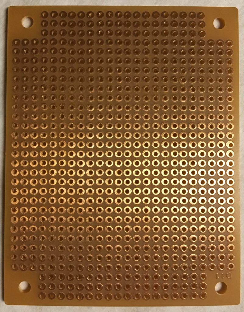
Most prototyping PCBs are terrible. What is it with boards like this one on the right? There are pads to solder the pins of each component to the board, but then how do you connect them? I’ve seen three options: one is to bend the leads of each component over to the component they should connect to and solder them. This ends up looking like a real old-school breadboard, like the kind that holds bread. Second, I’ve seen people drag a glob of solder across multiple pads to make a sort of trace from one pin to another. That takes a ton of solder and I can never get it to work. The third is to wrap wire around the leads of each component to make point-to-point connections. So if you want to solder everything twice, use that approach.

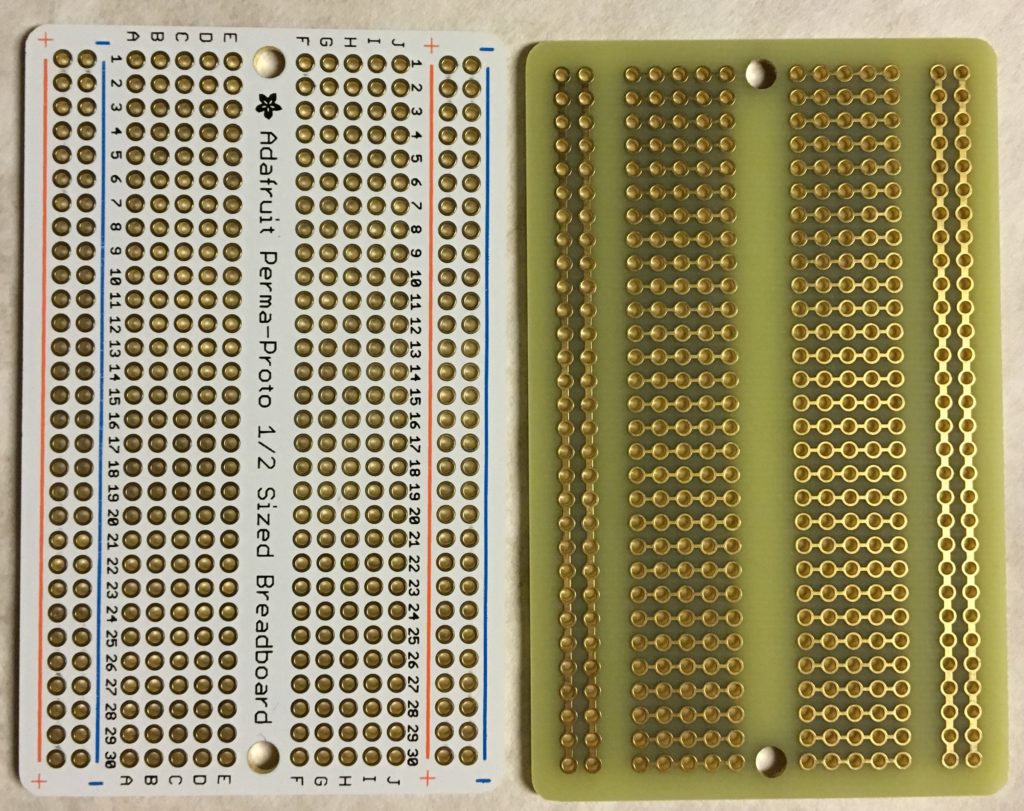
Here is a protoboard that doesn’t suck. Adafruit’s board is laid out exactly like a solderless breadboard and comes in three sizes. If you can lay your circuit out on a solderless breadboard, then you can solder it in here. The holes are plated through, so you won’t get lifted pads like you will with cheap single-sided boards. The bottom of the board (right) has no solder mask so you can cut the traces if you need to. That makes this a step up from a solderless breadboard in terms of versatility in layout.

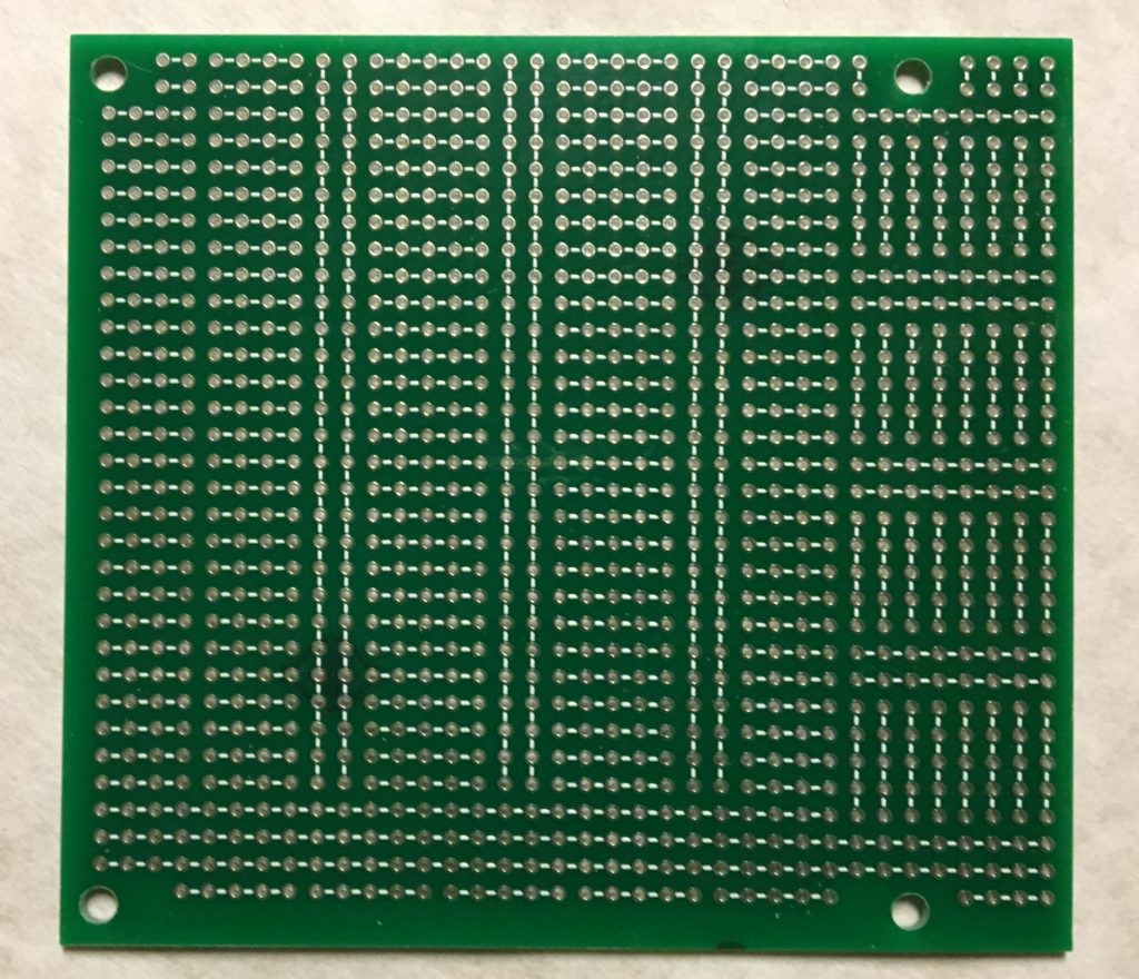
Here is my attempt at a protoboard, with several features I wanted. First, there is a place to put a two-row header at the top. Solderless breadboards don’t have a spot like that and it drives me nuts. Adafruit sells various breakout devices to accommodate the need. Second, I can lay out several chips in one row, two parallel rows, or some combination. Third, this board has mounting holes that match a commonly available enclosure I want to use! That is seriously rare for most protoboard. The two things that don’t work on this board are the area at the bottom, which was meant to accommodate tactile switches, and the holes throughout the board are too small for some components. Some diodes and resistors I want to use have fat leads and I didn’t account for that. So, on to version 2.0.